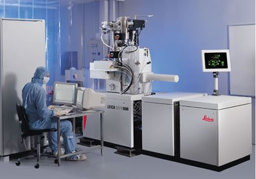
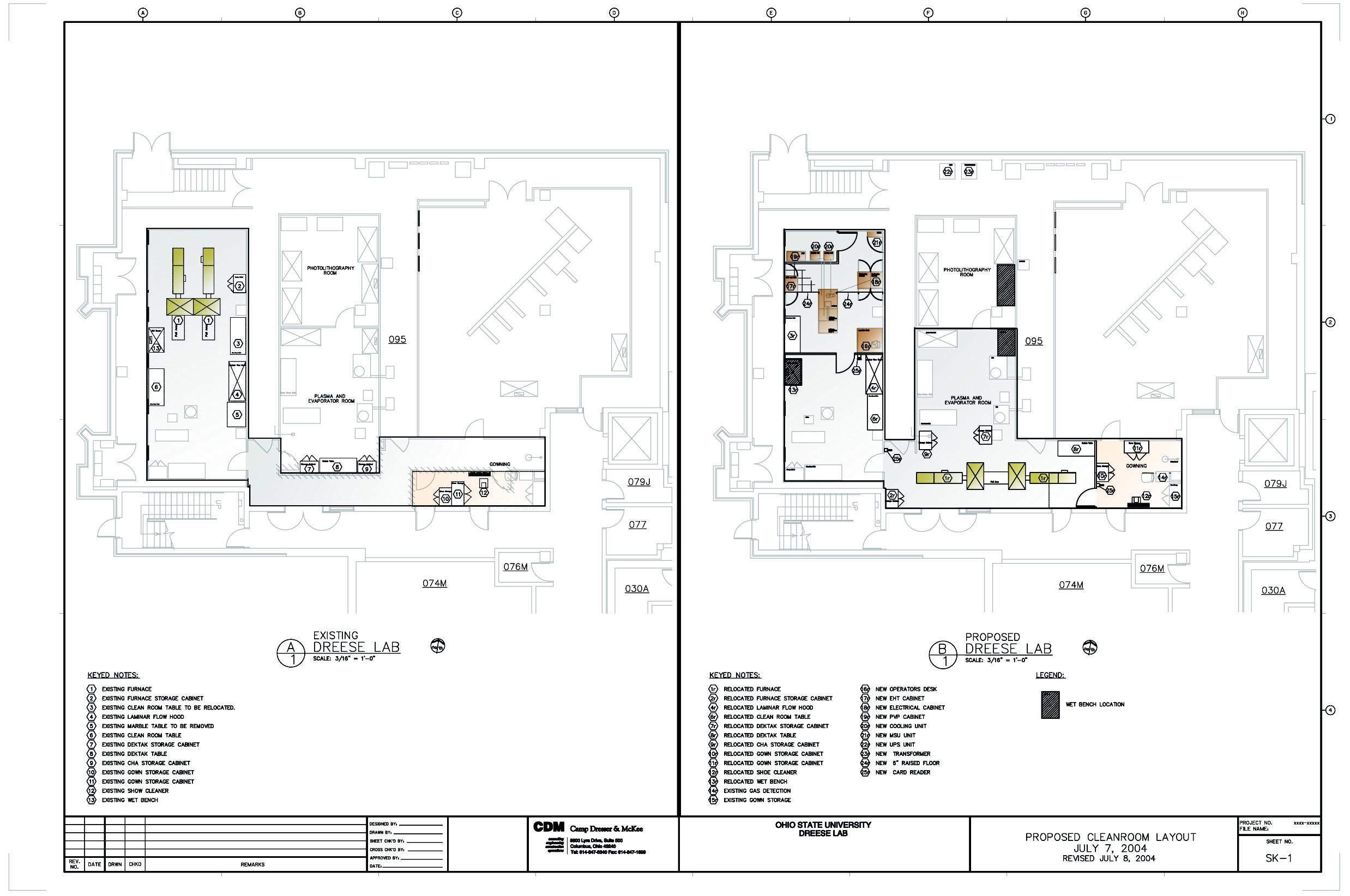
The Leica EBPG-5000 electron beam lithography system was delivered September 15, 2004. Renovations to the existing cleanroom are needed in order to complete the EBL installation. Our architect, Camp Dresser & McKee Inc., completed their design (see below) which provides for better cleanroom space utilization. Contractors were selected and work commenced in May 2005. The EBL was fully functional and officially accepted in January 2006, and cleanroom renovations were finalized in March 2006. The EBL system is now fully operational and open to internal and external users.

Below are a few images from the April 3, 2006 Kickoff Celebration.

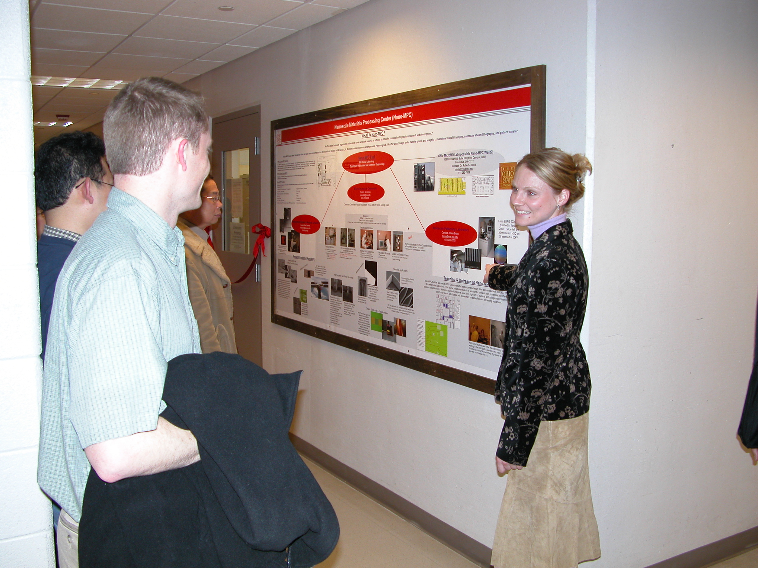

Please join us for the Kickoff Celebration of the new OSU Nanoscale Patterning Lab on April 3rd, beginning at 4:45 pm in 260 Dreese Lab on the OSU Campus ( Directions to 2015 Neil Avenue) and ending at 095 Dreese, outside the ECE Cleanroom.
In January 2006, the new multi-million dollar Nanoscale Patterning Laboratory opened its doors for business here at The Ohio State University, thanks to generous OBOR Hayes Investment Funding and significant support by the OSU Office of Research, College of Engineering and College of Math and Physical Sciences. At the heart of the laboratory is the Leica EBPG 5000 Electron Beam Lithography (EBL) system capable of a sub-10nm beam spot size. Users in the colleges of Engineering and Math and Physical Sciences have already begun taking advantage of the Laboratory, creating nanometer scale direct write patterns and high resolution photomasks in the first month.
Whether you are an active nanotechnology researcher, or just want to learn, come discover the nanotechnology opportunities that this new facility empowers. Talk with, and meet, the experienced staff to see how we may best work with you to meet your needs.
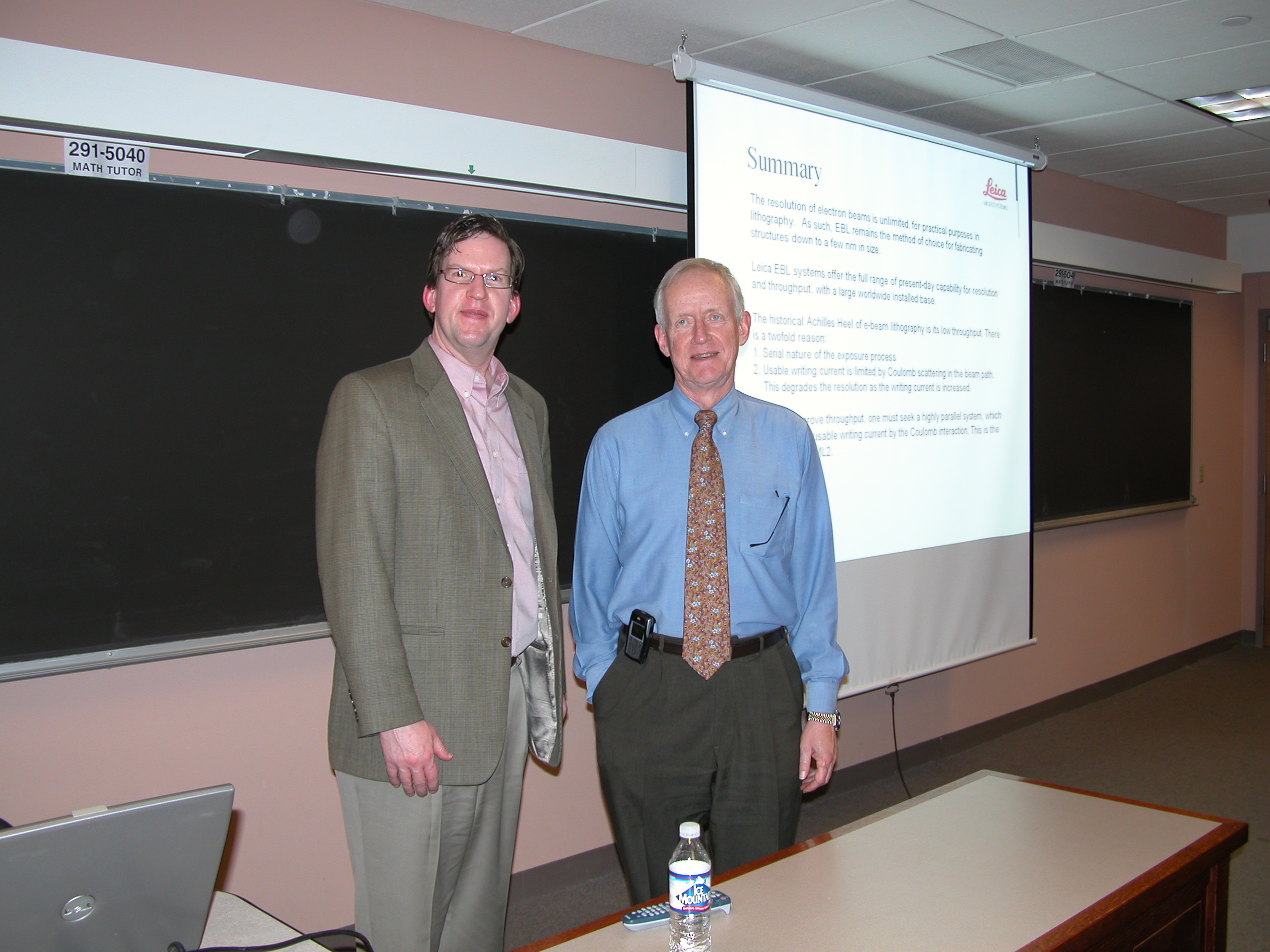
A keynote address from Dr. Timothy Groves of Leica Microsystems will
present a 1-hour seminar on The
State-of-the-Art in Electron Beam Lithography and Future Challenges" (PDF abstract).
A reception,  window tour of the lab (link to EBL room web camera), and ribbon cutting
will immediately follow.
window tour of the lab (link to EBL room web camera), and ribbon cutting
will immediately follow.
Please RSVP to Aimee (bross@ece.osu.edu) by March 31, and we look forward to seeing you there!
Sincerely,
Paul R. Berger, Director
Aimee L. Bross, EBL Engineer
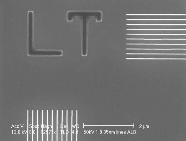
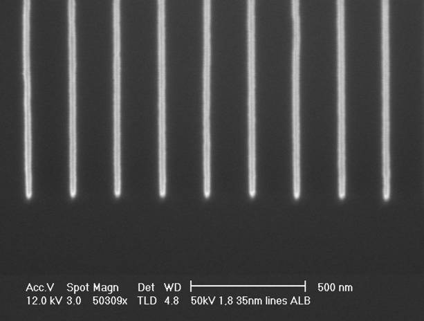
Below are early (12/19/05) photomicrographs of test patterns written during the tool acceptance testing.
Note, that the
field emission source permits a sub-10nm spot size, and thus we have not pushed the system to its lower resolutin limit yet.
Work to date has been at coarser resolutions only.
The Leica EBPG-5000 electron beam lithography system was delivered September 15, 2004. Renovations to the existing cleanroom are needed in order to complete the EBL installation. Our architect, Camp Dresser & McKee Inc., completed their design (see below) which provides for better cleanroom space utilization. Contractors were selected and work commenced in May 2005. The EBL was fully functional and officially accepted in January 2006, and cleanroom renovations were finalized in March 2006. The EBL system is now fully operational and open to internal and external users.
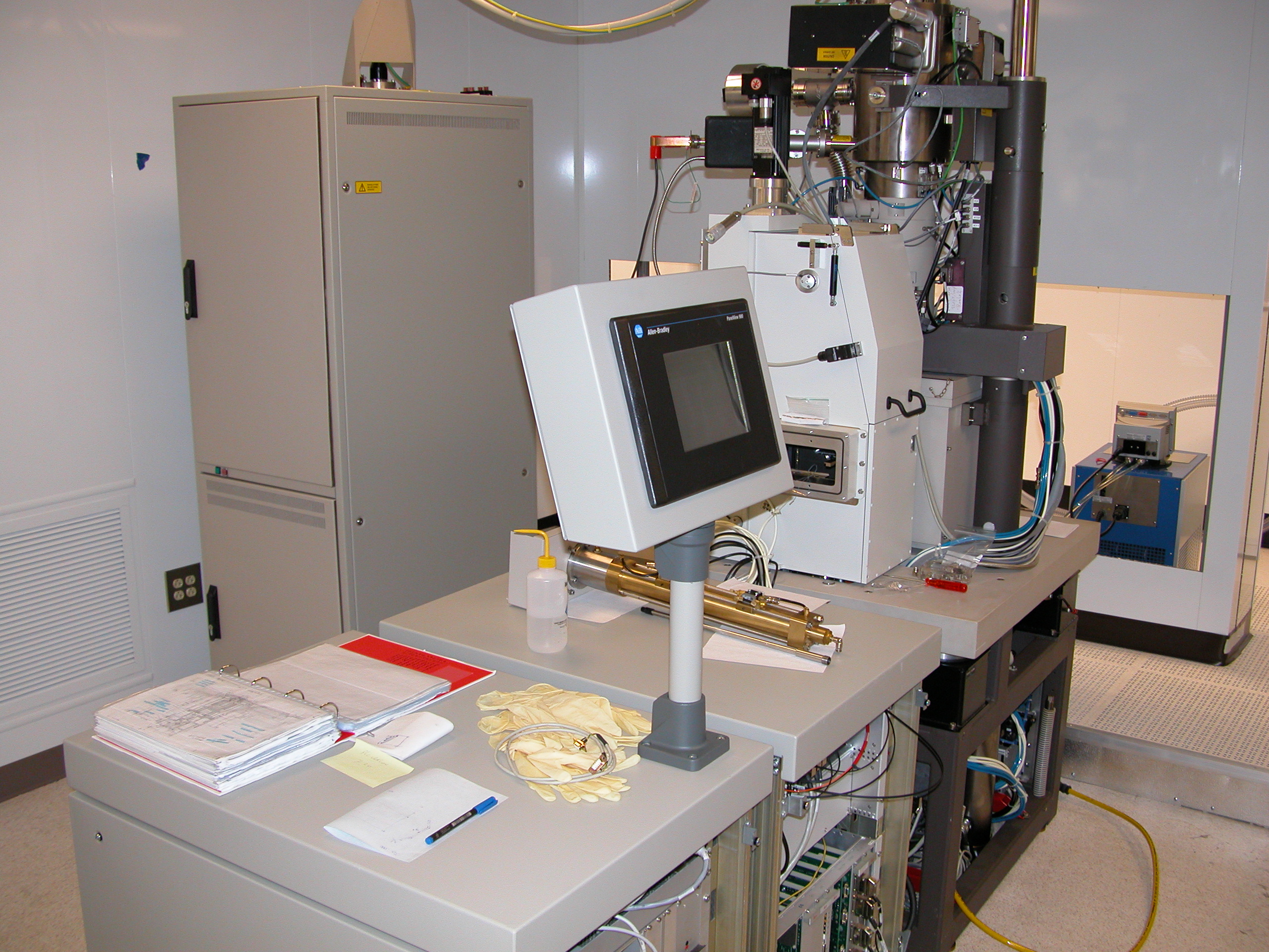
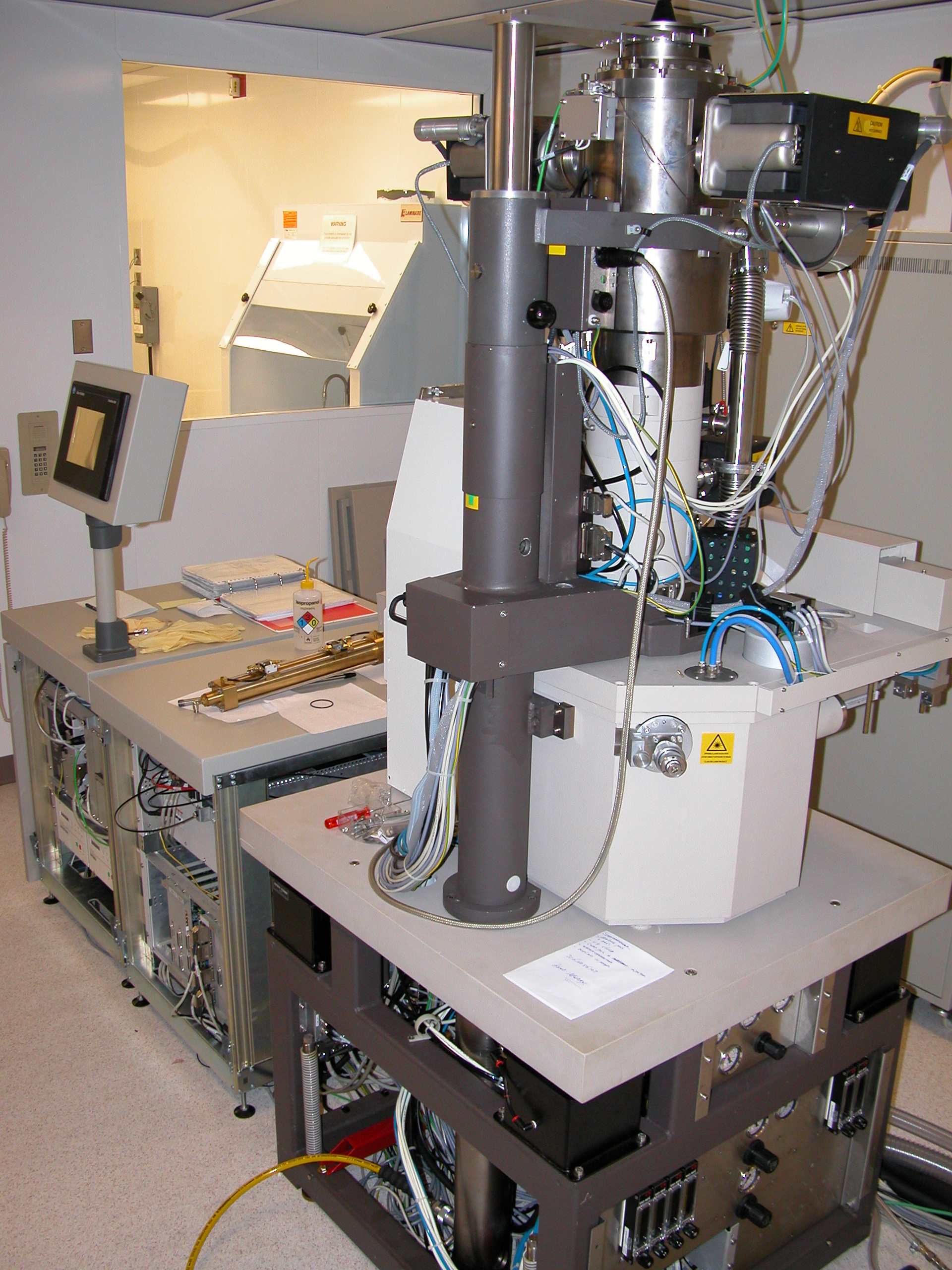
Below (left) is a picture of Room 095H Dreese Laboratory before construction. The furnaces were located in the space now occupied by the EBL tool. The tube furnaces shown were re-located to accommadate the EBL installation. Below (right) is an image from Leica of the EBPG-5000 EBL system just installed. Also below (bottom) is a CAD drawing of the cleanroom showing the prior configuration and the new design by Camp Dresser & McKee Inc., the architect for this project, which maximizes space utilization within the existing cleanroom space concurrently with functionality for semiconductor processing.

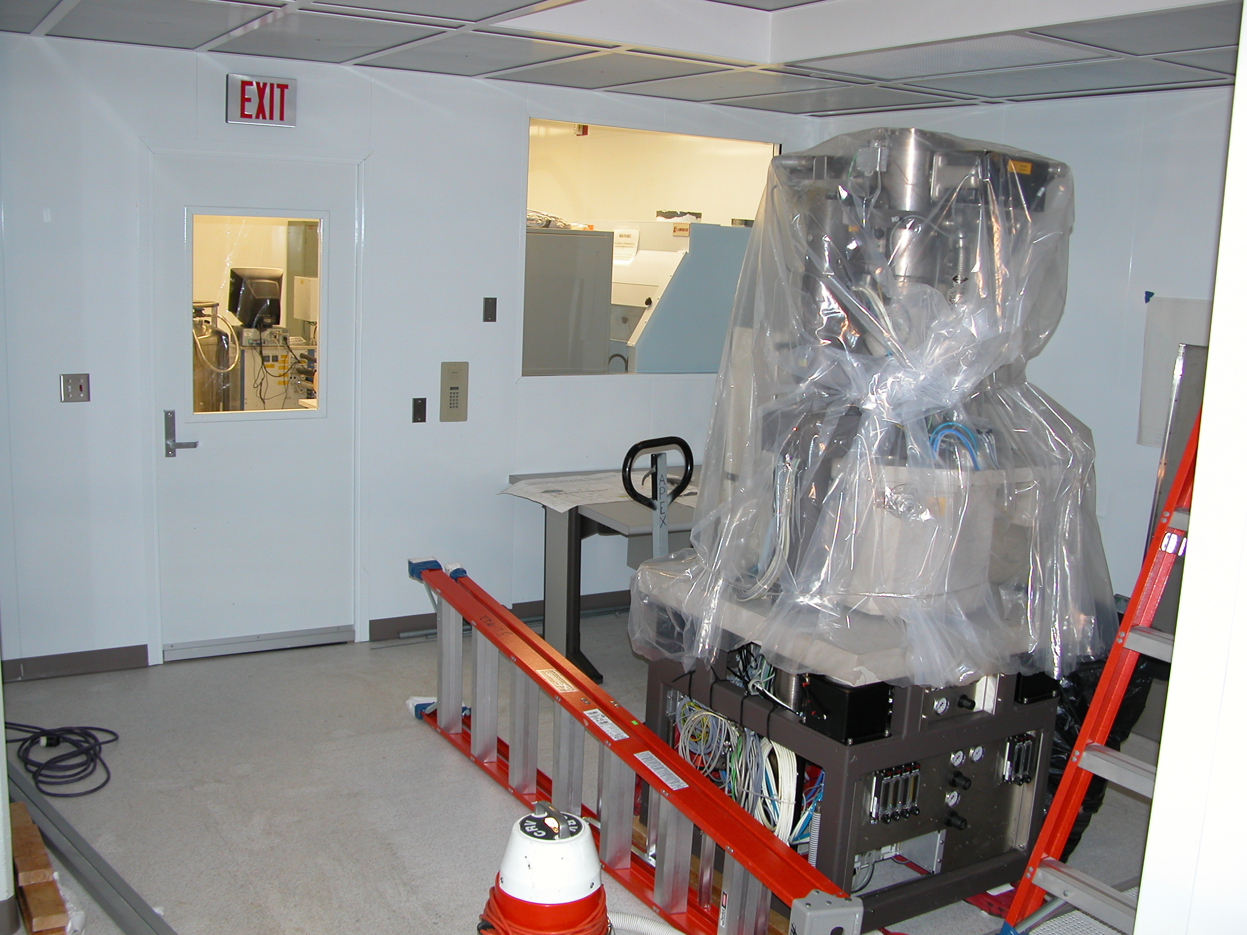
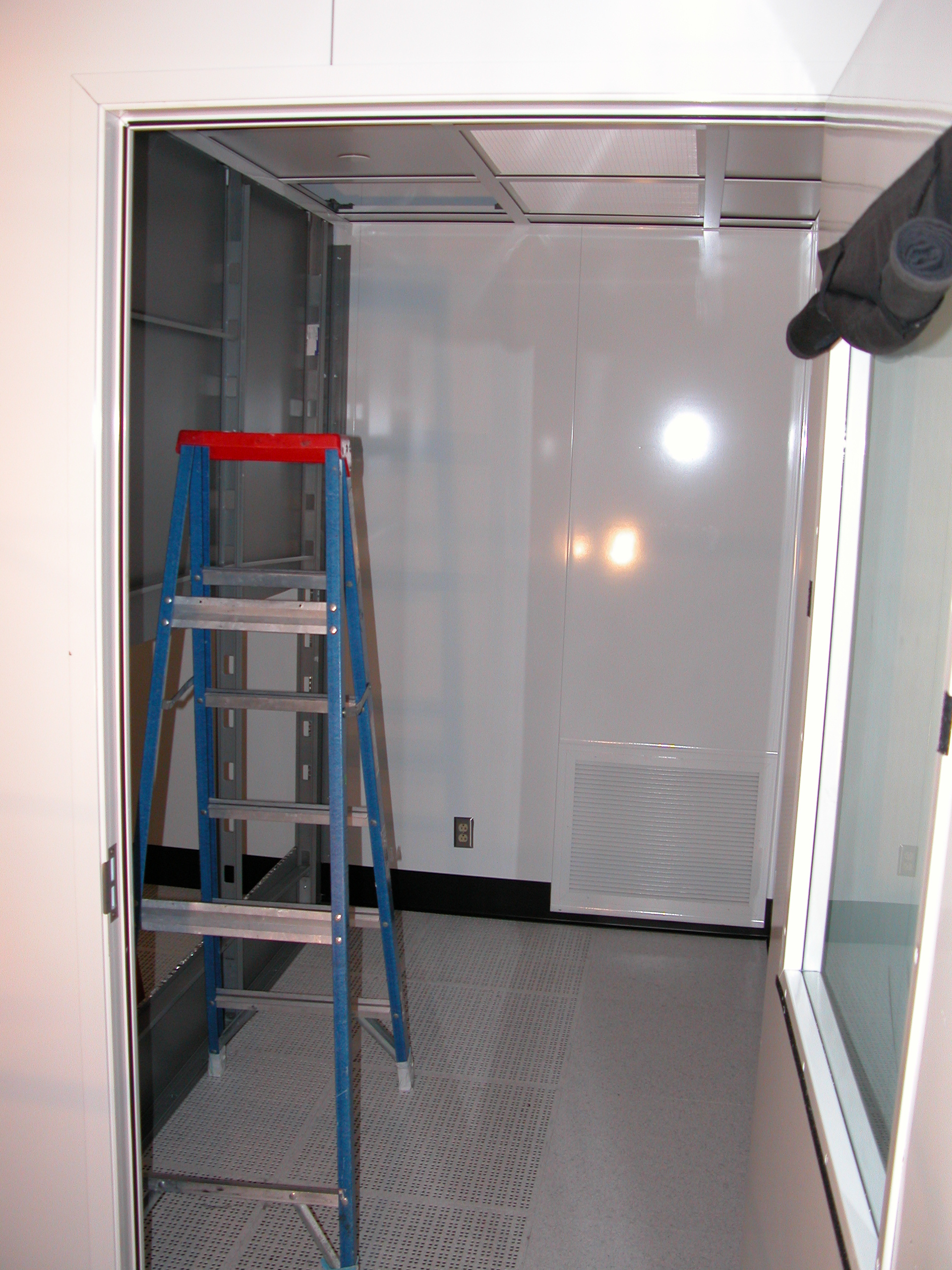
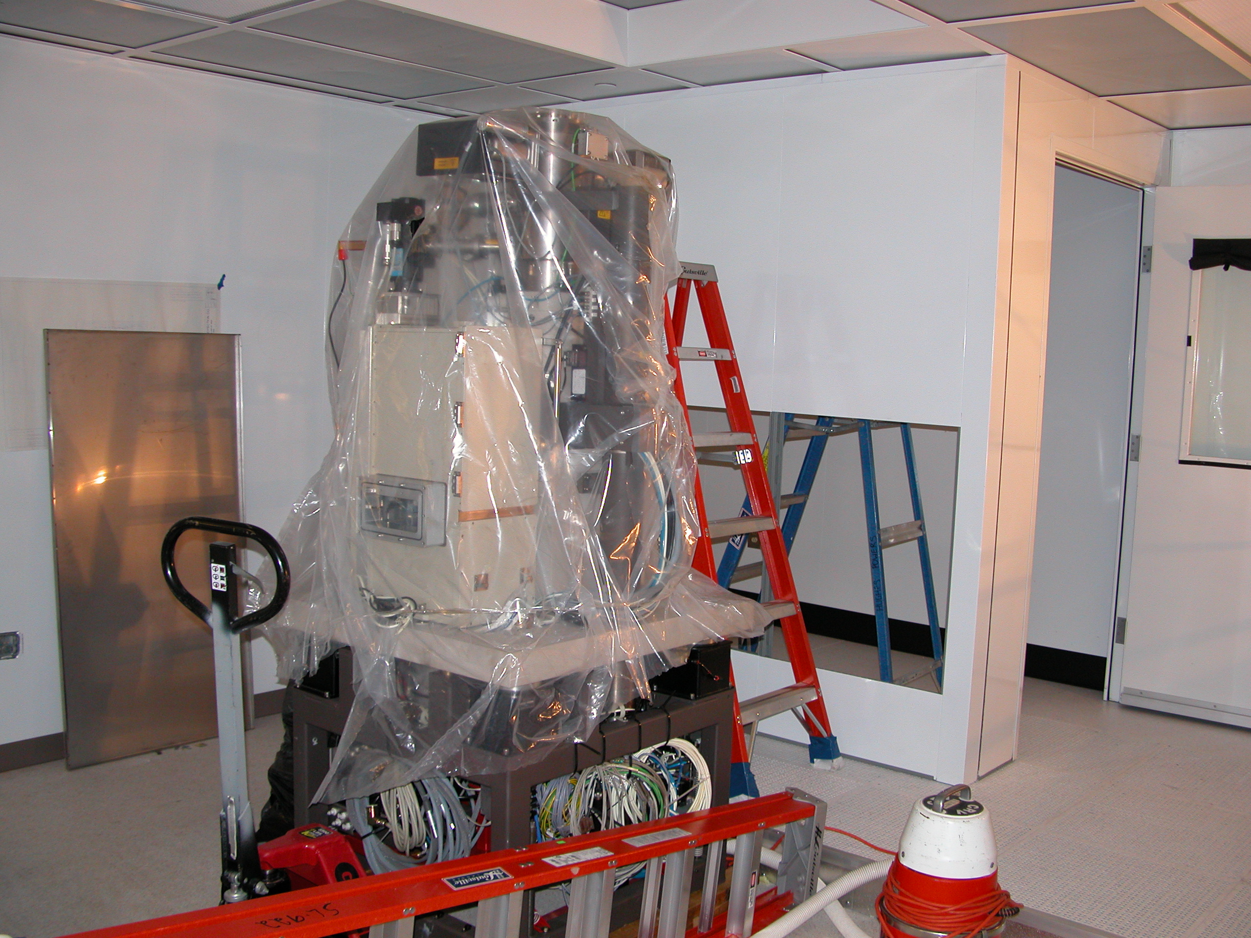
Below are a few photographs of the EBL lab space on October 2, 2005.
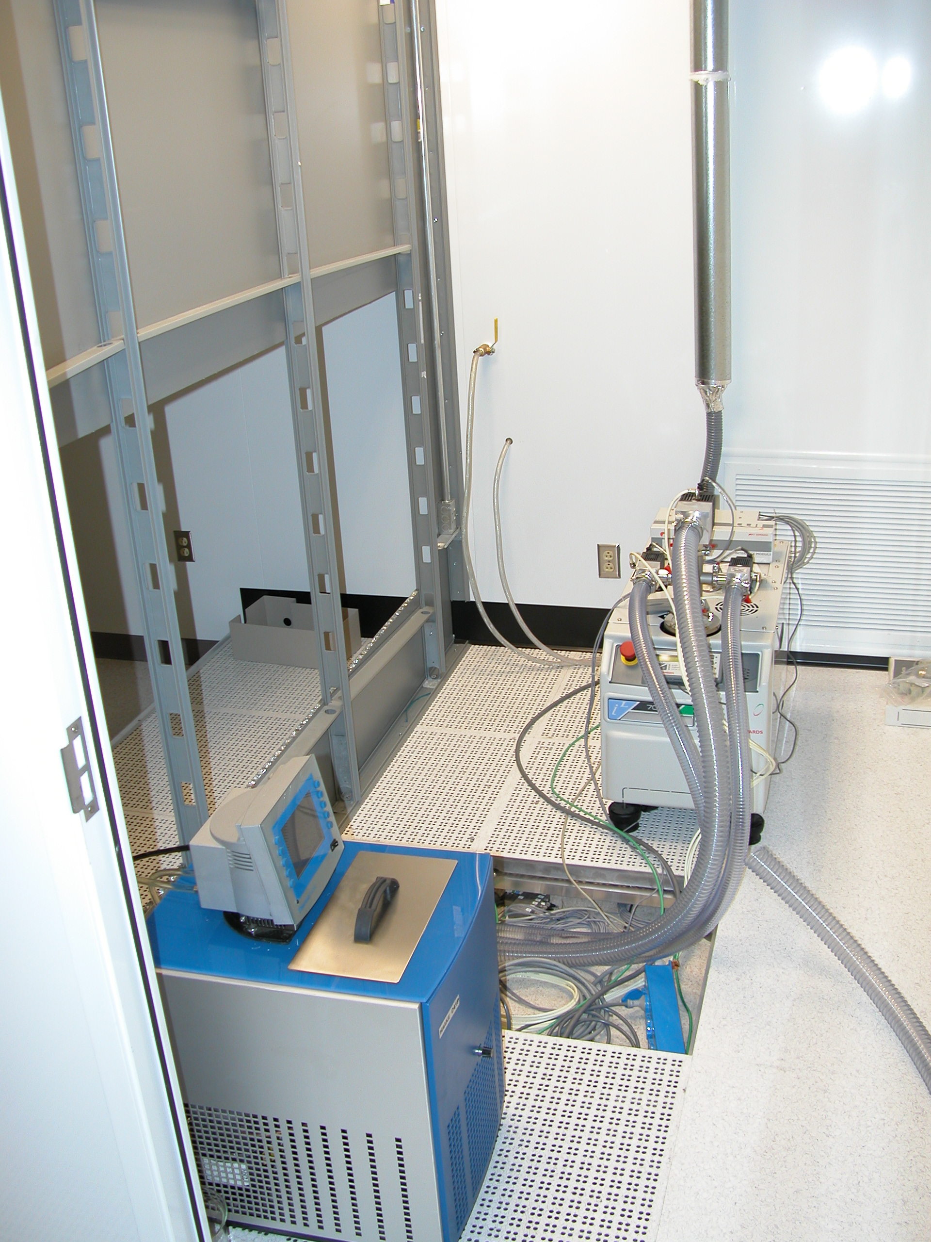
Below are a few photographs of the EBL lab space on September 1, 2005.
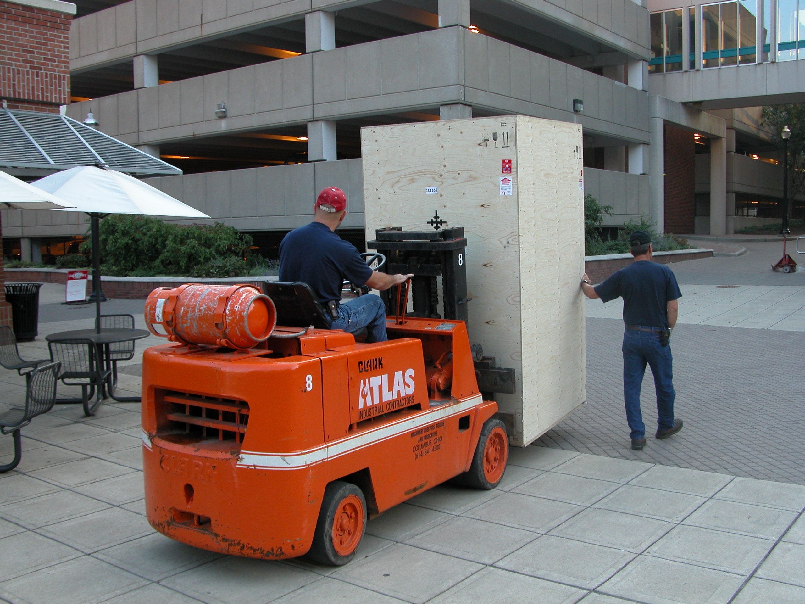
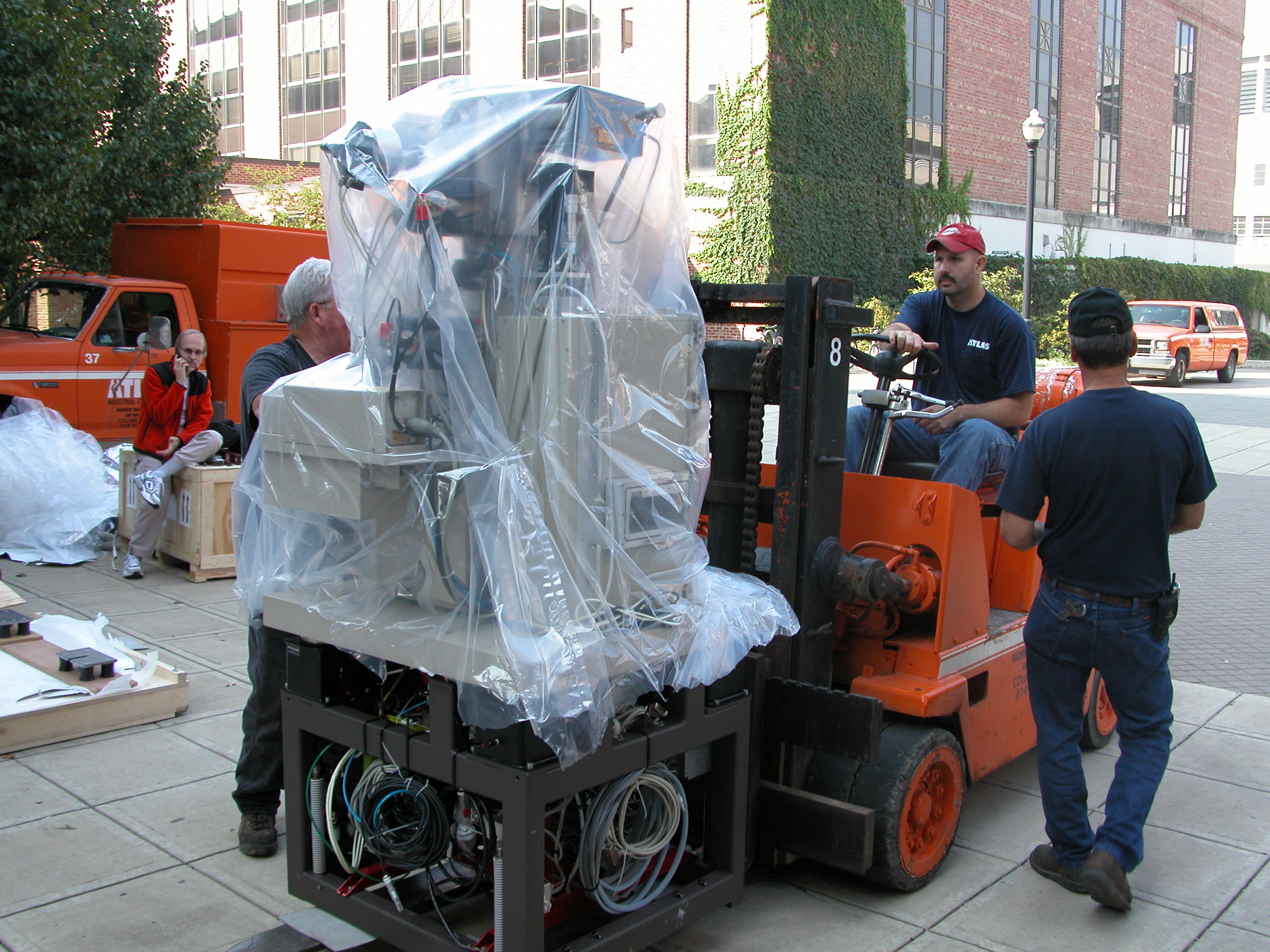
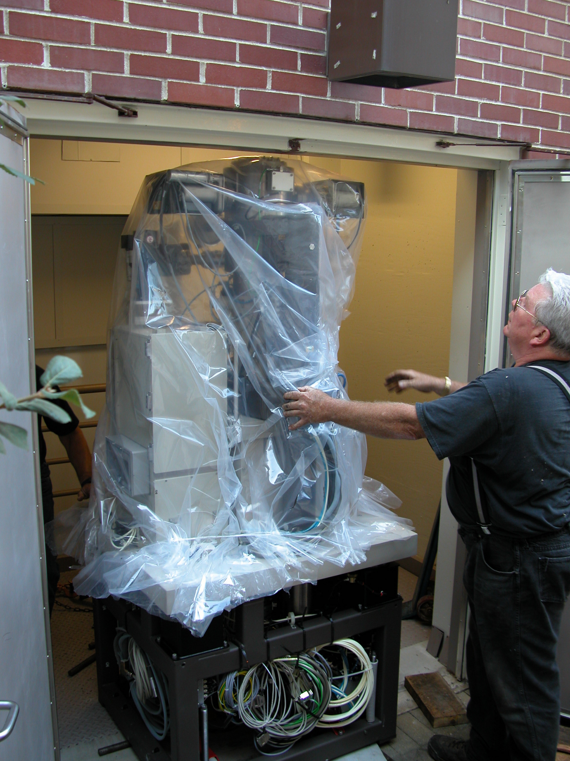
The new EBL system arrives and enters the cleanroom on September 15, 2004 (see photos below):